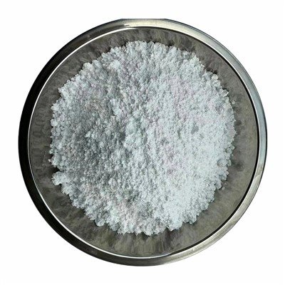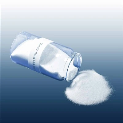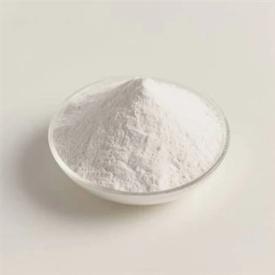

As a high-end inorganic non-metallic material, fused-grade silica powder plays an irreplaceable role in electronic packaging, integrated circuit substrates, high-temperature ceramics, and other fields. Its high purity (SiO₂ content ≥99.9%), low impurity content (Fe₂O₃ ≤0.01%), and high sphericity (≥90%) directly impact the thermal conductivity, insulation, and mechanical strength of end products. To meet the stringent requirements of downstream industries for material consistency and stability, a systematic solution requires comprehensive optimization across the entire supply chain, from raw material control and production processes to application adaptation.
The raw material requires carefully selected high-purity quartzite ore. XRF spectrometry and ICP-MS testing are used to remove transition metal impurities such as aluminum and titanium to ensure that the initial material purity meets standards. The fusion process utilizes an electric arc furnace or plasma fusion technology to heat quartz sand to above 1900°C to form amorphous silica powder. An inert gas atmosphere is used to prevent secondary contamination. Spheroidization is a key step. Through flame fusion or chemical vapor deposition (CVD) techniques, particle morphology is manipulated to increase packing density by 30%-40%, significantly improving filler flowability.
Solutions require customized solutions for different application scenarios: in epoxy molding compounds, particle size distribution (D50 = 1-5μm) needs to be optimized to balance thermal conductivity and stress; in copper-clad laminates, surface hydroxyl modification is required to enhance bonding with the resin. Furthermore, an SPC (Statistical Process Control) system is established to monitor key indicators such as particle size and whiteness in real time. In conjunction with ISO 9001 quality certification, batch stability tolerances of ≤0.5% are guaranteed.
In the future, with the advancement of the 5G communications and new energy vehicle industries, fused-grade silica powder will develop towards ultrafine (≤1μm) and low radioactivity (U/Th <1ppb). Collaborative innovation between industry, academia, and research to build a complete solution ecosystem, from basic materials to applied technologies, is the key path to breaking through material bottlenecks in high-end manufacturing.